← amare stover obituary remembering life amare stover update 2024 sandra atlas bass wikipedia life of sandra atlas bass photos and premium high res pictures →
If you are searching about How to Optimize a PCB Panel Layout - The Engineering Projects you've came to the right page. We have 25 Pictures about How to Optimize a PCB Panel Layout - The Engineering Projects like RF Design Guidelines PCB Layout and Circuit Optimization - Semtech | PDF, Practical Guidelines for High-Speed PCB Layout and Critical Component and also PCB Layout guidelines.pdf. Here it is:
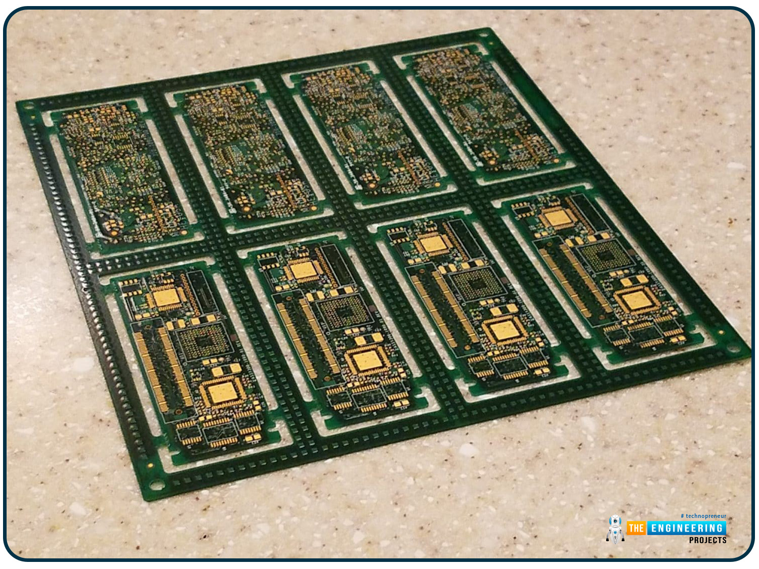
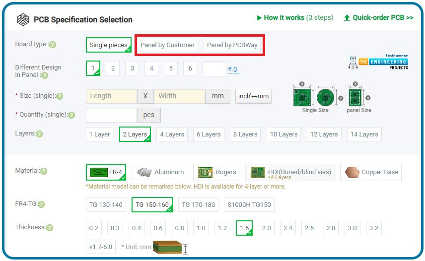
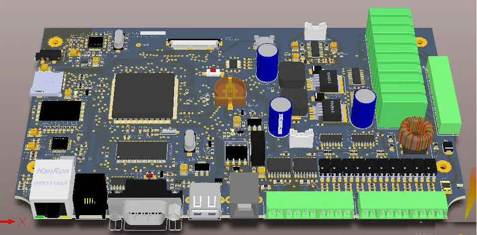
How To Optimize A PCB Panel Layout - The Engineering Projects
 www.theengineeringprojects.com
How to Optimize a PCB Panel Layout - The Engineering Projects
The Top 5 PCB Design Guidelines For Analog Circuits
 resources.pcb.cadence.com
The Top 5 PCB Design Guidelines for Analog Circuits
How To Optimize A PCB Panel Layout - The Engineering Projects
 www.theengineeringprojects.com
How to Optimize a PCB Panel Layout - The Engineering Projects
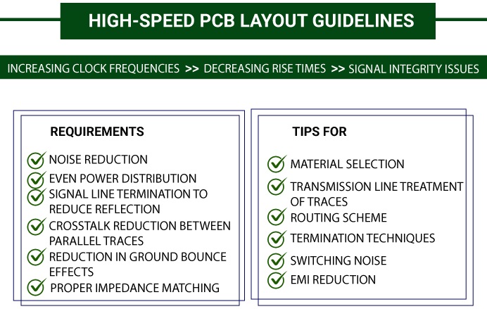
High Speed Pcb Layout Guidelines - Design Talk
 design.udlvirtual.edu.pe
High Speed Pcb Layout Guidelines - Design Talk
PCB Layout Guidelines | Design Rules & Requirements | Tips
 www.wellpcb.com
PCB Layout Guidelines | Design Rules & Requirements | Tips
Practical PCB Design Layout Rules - Leading PCB Manufacturer - Arisentec®
 arisentecpcb.com
Practical PCB design layout rules - Leading PCB Manufacturer - Arisentec®
PCB Layout & Circuit Analysis Techniques
 www.wizlogix.com
PCB Layout & Circuit Analysis Techniques
RF Design Guidelines PCB Layout And Circuit Optimization - Semtech | PDF
 www.scribd.com
RF Design Guidelines PCB Layout and Circuit Optimization - Semtech | PDF
Pcb Layout Guidelines For Decoupling And Bypassing Ca - Vrogue.co
 www.vrogue.co
Pcb Layout Guidelines For Decoupling And Bypassing Ca - vrogue.co
PCB Layout Design Services | Circuit Board Design | Optimum
 www.optimumdesign.com
PCB Layout Design Services | Circuit Board Design | Optimum
A Detailed Guide To PCB Layout Design - IBE Electronics
 www.pcbaaa.com
A detailed guide to PCB layout design - IBE Electronics
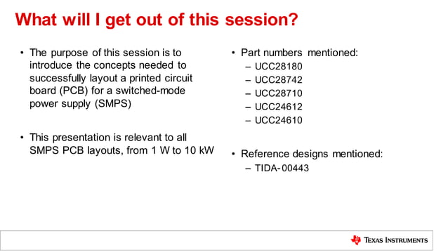
(PDF) PCB Layout Guidelines For Power Controllers - TI. · PDF FilePCB
 dokumen.tips
(PDF) PCB Layout Guidelines for Power Controllers - TI. · PDF filePCB ...
PCB Layout Guidelines.pdf
 www.slideshare.net
PCB Layout guidelines.pdf
Help For PCB Layout Quality, Improvements, Fixes.
 home.fedevel.com
Help for PCB Layout quality, improvements, fixes.
How To Design PCB Layout? - Guidelines, Advantages And Disadvantages
 compuinfohub.blogspot.com
How to Design PCB Layout? - Guidelines, Advantages and Disadvantages ...
How To Optimize A PCB Panel Layout - The Engineering Projects
 www.theengineeringprojects.com
How to Optimize a PCB Panel Layout - The Engineering Projects
BASIC PCB Design Rules – Layout
 epci.eu
BASIC PCB Design Rules – Layout
PCB Layout Optimisation | PDF | Electrostatic Discharge | Printed
 www.scribd.com
PCB Layout Optimisation | PDF | Electrostatic Discharge | Printed ...
PCB Layout Guidelines.pdf
 www.slideshare.net
PCB Layout guidelines.pdf
PCB Layout Design Best Practices Guidelines & Software
 www.electronicsforu.com
PCB Layout Design Best Practices Guidelines & Software
PCB Design & Layout Skills – PCB Manufacturing And PCBA Assembly
 www.grande-pcba.com
PCB Design & Layout Skills – PCB Manufacturing and PCBA Assembly ...
How To Optimize A PCB Panel Layout - The Engineering Projects
 www.theengineeringprojects.com
How to Optimize a PCB Panel Layout - The Engineering Projects
PCB Layout Guidelines.pdf
 www.slideshare.net
www.slideshare.net
PCB Layout guidelines.pdf
PCB Layout Guidelines For High Speed Applications – PCB HERO
 www.pcb-hero.com
PCB Layout Guidelines For High Speed Applications – PCB HERO
Practical Guidelines For High-Speed PCB Layout And Critical Component
 www.scribd.com
Practical Guidelines for High-Speed PCB Layout and Critical Component ...
How to optimize a pcb panel layout. Basic pcb design rules – layout. How to optimize a pcb panel layout